Setting the Standard for Industry 4.0
Uncovering TSMC’s Two Special Weapons
Source:TSMC
TSMC has revealed its smart manufacturing weapons for the first time. In an exclusive interview with CommonWealth, a top TSMC executive explains how the semiconductor powerhouse has used AI and machine learning to make chips faster than anybody else and achieve consistency across its 13 fabs.
Views
Uncovering TSMC’s Two Special Weapons
By Jimmy HsiungFrom CommonWealth Magazine (vol. 665 )
Major manufacturing powers around the globe have moved aggressively to dominate the world of smart manufacturing. So it may be surprising to some that the benchmark for Industry 4.0 can be found in Taiwan – semiconductor giant Taiwan Semiconductor Manufacturing Company (TSMC).
The wafer manufacturing sector is widely acknowledged to require more advanced and complex production technology than any other field, and TSMC has established itself within the sector as a clear technology leader, especially since it began churning out chips using its 7-nanometer process in 2018. Critical to that success are capabilities the company has only now decided to disclose.
In this in-depth look at the world’s largest contract chipmaker that we hope will provide insight on the mesmerizing might of “smart” factories and give added impetus to Taiwan’s digital transformation, CommonWealth Magazine chronicles TSMC’s smart manufacturing journey that has propelled it to dominance in the contract wafer field.
TSMC’s Secrets Revealed for the First Time
Fully Automated 19 Years Ago
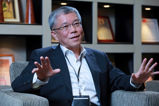
“We have talked about manufacturing excellence from the day we were founded. It’s a value we want to highlight,” says J.K. Wang, TSMC’s senior vice president for fab operations.
As TSMC’s wafer production czar, Wang is the company’s most senior executive involved in smart manufacturing. As he discussed the company’s secret weapons in its “smart” arsenal, he belied the stereotypical image of the brusque production line manager, speaking eloquently of TSMC’s journey from the very beginning. (Read: 'Queen of Wafers' Doris Hsu: The Women to Watch in Asian Tech)
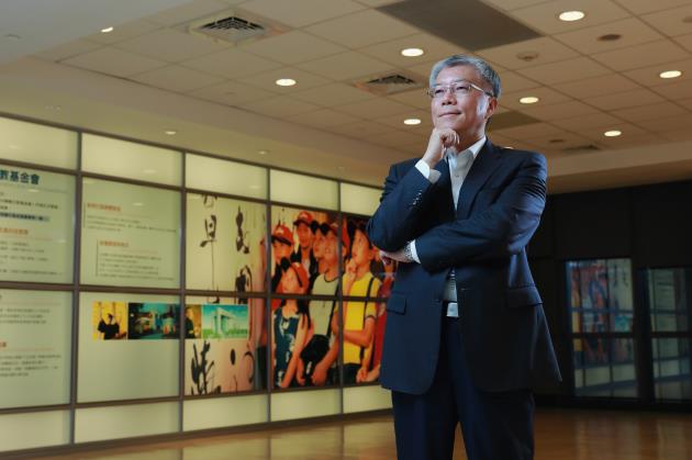 J.K. Wang, TSMC’s senior vice president for fab operations, is considered the company’s smart manufacturing “soul.” (Source: Chien-ying Chiu)
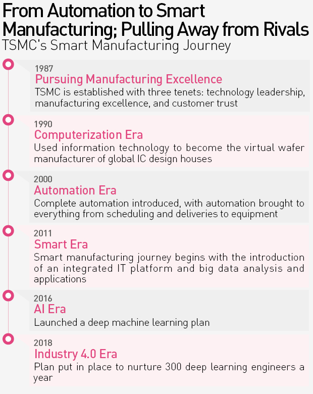
Wang, whose TSMC employee number is 30, has been with the company since its founding in 1987 and participated in its relentless pursuit of manufacturing excellence since. TSMC first set a threshold for production management in the 1990s, he says, when its 8-inch wafer introduced computerization.
Automation began in earnest in 2000 when TSMC built a massive 12-inch wafer fab whose degree of automation surpassed that of any of its rivals’ facilities. From scheduling jobs and deliveries to the fab’s equipment, the operation was virtually fully automated. (Read: Snatching Apple Orders: TSMC’s Unsung Weapon)
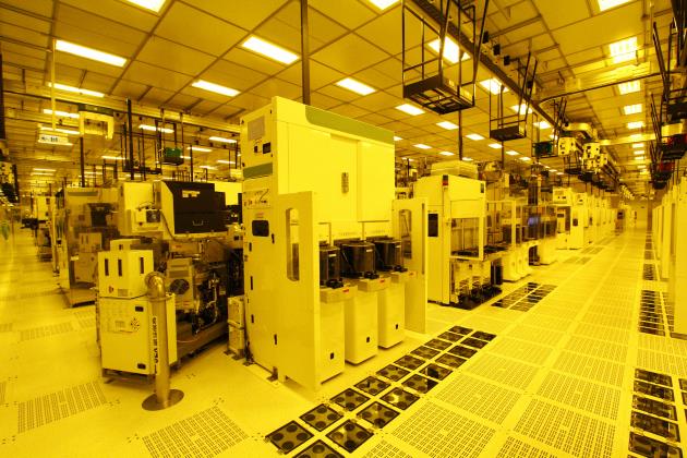
The work environment at a TSMC fab today more than ever defies conventional images of a semiconductor factory. That became clear when CommonWealth reporters entered the MCC (manufacturing control center) on a visit to TSMC’s 12-inch wafer fab in the Central Taiwan Science Park.
There was no need to change into dust-free garments or pass through an air shower. Casually dressed engineers and technicians sat in neatly lined rows, their eyes focused on their computer screens scanning all types of data. Through the office’s huge windows, Dadushan was visible in the distance under the blue sky and white clouds.
 TSMC is changing the sanitized image of wafer fabs. Engineers and technicians can command the production process from the MCC (manufacturing control center). (Source: TSMC)
“Technicians all work outside the factory. The aisles in the factory itself are completely empty, and the chips are automatically conveyed,” Wang says, noting that people only appear on the production line to perform protective maintenance on the machines.
“Today, everybody can dress themselves up. In the past, they couldn’t even wear makeup,” he says.
Leading the ‘Smart’ Charge 8 Years Ago
Applying AI, Machine Learning to Making Wafers
But even today, TSMC is finding ways to make automation ever more sophisticated.
“Every batch of goods knows where its next stop will be. Every machine knows what the next batch of goods will be. The entire process works smoothly, but the key is that it must be tight,” Wang says.
Comparing the process to a physical checkup, Wang explains that the most time consuming part of a physical is the time spent waiting between different tests, something he sees as terribly inefficient. The wafer manufacturing process has three stages – queue time, hold time and run time – and though TSMC has shortened the first two stages to an absolute minimum in recent years, Wang insists in a resolute tone that the company is striving for a production line that never stops.
The stage for this foray into smart manufacturing was set by the company’s growing mastery of automation. In 2011, TSMC raised the curtain on a smart wafer foundry, and it has since added several key technologies to the mix, including big data analysis, machine learning, and artificial intelligence, that provide valuable information on the process.
Wang describes semiconductor manufacturing as a highly complex craft involving more than 1,000 steps that must be precisely controlled performed in factories with thousands of machines that collect millions to tens of millions pieces of data a day. (Read: Germany's Industry 4.0 Strategy)
This data reflects every detail that goes into producing a wafer and must be fully compiled and mastered before the process’s parameters can be optimized, which is at the heart of elevating the yield rate, Wang says.
Chen-fu Chien, a distinguished professor in National Tsing Hua University’s Department of Industrial Engineering and Engineering Management, says every TSMC wafer generates a million points of data, and every foundry has thousands of pieces of equipment, but the company employs fewer than 1,000 process engineers. Analyzing such mountains of data has clearly surpassed human capabilities and become an art in itself.
According to Chien, standard commercial statistics software can support big data analysis, but because every sector has its own specialized needs and features, and an industry leader such as TSMC will typically develop proprietary analytical tools consistent with its own specific requirements.
Enter TSMC’s 1,000 IT and 300 AI and machine learning engineers. With their help, TSMC has developed smart diagnosis engine and advanced analytics platforms over the past few years that have supported the creation of a unique manufacturing precision control system.
This know-how, involving the application of big data and machine learning to wafer production, can be seen as TSMC’s decisive secret edge in widening the distance between it and its global competitors.
 Source: Jimmy Hsiung
Unique Weapon 1: Reducing the Cycle Time
Unrivaled Lead Times
So how effective has the system been? It has reduced what former TSMC Chairman Morris Chang called the industry’s most important number: cycle time.
Understanding “cycle time” requires a general understanding of the chip manufacturing process. Simply put, TSMC’s job is to take the circuit drawings submitted by clients (IC design companies) and fit those circuits on chips the size of a finger nail. Aside from holding the width of the circuit’s lines to 1/10,000th of the diameter of a hair, TSMC must also create and stack layers in a chip as though erecting a building.
Each layer goes through exposure, development, ion implantation and etching processes to be able to pack circuits with more than 1 billion transistors on each layer. The cycle time refers to the time it takes to build each layer.
As the life cycles of consumer electronics products continue to get shorter, “lead times [even more than yield rates and prices] are our highest priority, and in that area, TSMC is indeed the best,” says a top executive at an IC design house.
A key factor in TSMC’s unbeatable lead times is the competitiveness of its cycle time. Wang reveals that the company’s cycle time has improved by at least 50 percent since it began adopting smart manufacturing practices and applying big data and machine learning.
Because TSMC’s rivals and clients have wanted to uncover the secrets beyond the company’s prowess, Wang was still very tight-lipped on the details and specific numbers related to different processes. As early as 2017, however, then TSMC co-CEO C.C. Wei disclosed in a speech at the company’s Technology Symposium in Taiwan that the goal of applying big data and machine learning to process management “was to lower our cycle times.”
Wei said that roughly 15 years earlier during the 180nm era, a chip had about 25 layers, and each layer took about two days to make. By 2017 when he gave his speech, however, a 10nm mobile phone chip had 80 layers, meaning that if the cycle time of each layer was still two days, the chip would have taken nearly six months to produce. “Nobody can wait that long,” Wei admitted at the time. (Read: Big Money ≠ A Second TSMC)
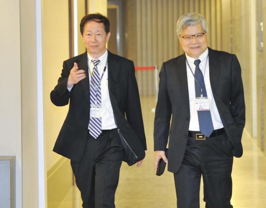 After taking over from former Chairman Morris Chang, TSMC Chairman Mark Liu (left) and Vice-Chairman and CEO C.C. Wei (right) accelerated the company’s smart manufacturing program. (Source: Kuo-Tai Liu)
Unique Weapon 2: Fab Matching
Precision Manufacturing and Optimization
As it moved into the smart wafer manufacturing era, TSMC had another essential unique weapon: consistency across all of its fabs, a model it calls “fab matching.”
In his new book “Industry 3.5,” National Tsing Hua University’s Chien wrote that an analysis of machine parameters and data from sensors enables more than just real-time predictions on the quality of each processed product. It also allows machines to act “intelligently,” giving them the ability to do self-testing, adjust process parameters, reset automatically, and improve controls – what Chien calls “dynamic rolling optimization.” Through this process of constant diagnosis, feedback and learning, machines become increasingly smarter.
Even more impressively, it ensures that nobody “is distanced” from the team during the process.
In the semiconductor industry, when companies get ready to mass-produce a new chip, they first have their R&D department put it through a trial run. Only when production parameters and other factors have been adjusted to their optimal levels is the chip sent out to different fabs to produce in large volumes.
The process is similar at TSMC, which has 13 fabs around the world. Wang says the company generally has its main foundry conduct the necessary tests until the process is considered stable before the chip can be turned over to one of the fabs for mass production.
Precisely replicating the results obtained in the trial runs when shifting to mass production, however, often represents a major challenge for most semiconductor makers. The best known model in the past was Intel’s “Copy Exactly” methodology.
It meant that every production line in every Intel wafer fab around the globe used the same production equipment and each factory’s flow and configuration, dimensions, length and even corners were identical. Not only did it ensure uniformity between test runs and mass production, it also prevented the same problems from recurring.
 J.K. Wang says optimization is par for the course at TSMC. This capability has enabled TSMC to build a cost threshold that rivals are hard-pressed to overcome. (Source: Chien-ying Chiu)
TSMC uses a similar model, its “fab-matching.” But the adoption of “smart” processes has given TSMC an extra flexibility that competitors simply cannot imitate.
As Wang explains it, fab-matching involves more than simply ensuring that the same process can be identically replicated in any of TSMC’s fabs. It also means that if a production process in one fab generates better process parameters or higher yields or drives the use of a more cost-efficient machine, other fabs will realign themselves with the new findings.
“People normally aren’t willing to touch a thing once mass production begins,” but at TSMC, continuing to optimize the process is par for the course, Wang says.
What Wang didn’t say is that this capability alone has enabled TSMC to create a cost threshold that rivals are hard-pressed to overcome.
Adhering to an insistence on manufacturing excellence that has turned it into a global manufacturing model, TSMC has grabbed the world’s attention. Now, that world will is watching to catch TSMC’s next “smart manufacturing” act.
Translated by Luke Sabatier
Edited by Sharon Tseng
Views

Subscribe to CWE Newsletter (every Thursday)
Stay abreast of what's happening in Taiwan with our weekly digest.