The Japan-Taiwan semiconductor island chain
Source:Elaine Huang
TSMC recently opened a new wafer fab in Japan, igniting a new era of semiconductor cooperation between Japan and Taiwan. What motivated TSMC to expand into Japan, and how could this new “island chain” affect the global semiconductor market?
Views
The Japan-Taiwan semiconductor island chain
By Elaine HuangFrom CommonWealth Magazine (vol. 793 )
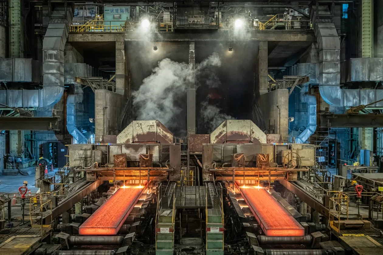
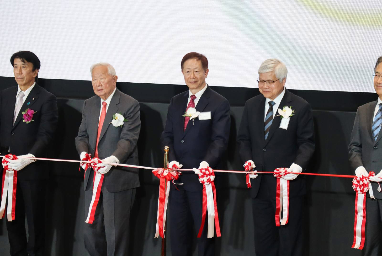
When TSMC opened a 12-inch wafer fab in Kumamoto on February 24, a “3-hour semiconductor island chain” linking Taiwan and Japan took shape. It is a partnership poised to do battle with the United States and China in the chip war of the future in a world in which semiconductors represent national power.
The contours of this future war had already begun to take shape a few years ago. A technology “Cold War” between Washington and Beijing bubbled to the surface in 2020, the same year the U.S. passed the CHIPS Act, highlighting the central role semiconductors play in national security and resilient supply chains.
Japan’s Ministry of Economy, Trade and Industry (METI) has also gotten into the act, launching a semiconductor promotion initiative that provided a subsidy of ¥470 billion (about US$3.15 billion) to TSMC to build its first Kumamoto fab as well as spawned a home-grown chipmaker called Rapidus. Through a partnership with IBM, Rapidus is determined to leave behind Japan’s backward 40-nanometer process technology and achieve mass production of 2nm logic chips by 2027.
Leveraging TSMC is another key component of the Japanese government’s plan to revitalize its chip industry.
“I hope it can be successful. I’ll support it,” stressed Japanese semiconductor pioneer Tsugio Makimoto (牧本次生), who is now in his 80s. “Having a TSMC fab in Japan is very important because Japan knows it’s not enough to depend only on yourself.”
TSMC’s Kumamoto factory, a joint venture named Japan Advanced Semiconductor Manufacturing Inc. (JASM), is located in the town of Kikuyo, about half an hour away from Aso Kumamoto Airport on the southern island of Kyushu.
Kyushu has a special place in Japanese history. At the end of Japan’s shogunate period, it was at the heart of Japan’s Westernization and opening to the world, and it bought steam ships and established a navy on its own. Kyushu natives Takamori Saigo (西鄉隆盛) and Toshimichi Okubo were key figures in Japan’s Meiji Restoration.
In the 1980s, Japanese semiconductor companies such as NEC, Mitsubishi Electric and Tokyo Electron Ltd. flocked to Kumamoto to set up shop and were instrumental in forging “Silicon Kyushu,” which propelled Japan’s rise to the top of the global semiconductor sector.
Pushing Ahead of the United States
TSMC’s move to Kumamoto was largely driven by the strong support of Japan’s government.
Wanting to revive Japan’s semiconductor sector after 30 years of decline, then Japanese Prime Minister Shinzo Abe (安倍晉三) introduced a national semiconductor revitalization policy that in 2020 set the goal of seizing a 20 percent share of the global chip market by 2030. Part of the plan was to solicit TSMC investment.
That aggressive posture explains why, while the U.S. government continues to drag its feet in subsidizing TSMC’s new fab in Arizona, the Japanese government’s ¥470 billion subsidy for the first TSMC fab in Kumamoto has already been paid in full.
On the day TSMC opened that complex, the Japanese government also announced that it would provide an additional ¥732 billion to TSMC for its second, more advanced fab in Kumamoto.
Japanese lawmaker Akira Amari (甘利明), known in his home country as the “chip czar,” said in an interview with CommonWealth Magazine last year that the subsidy for the TSMC fab was not only the Japanese government’s first given to a specific industry but also the biggest ever granted to a single foreign enterprise.
Wouldn’t so much money going to an outsider trigger resentment among Japanese companies?
“Japan needs the capabilities of high-end logic chip manufacturers, otherwise it will be controlled by others. Japan needs TSMC,” the 74-year-old Amari responded without hesitation.
Few Kyushu residents had ever heard of TSMC three years ago. But after the world’s largest contract chipmaker set up JASM in Kumamoto in 2021 and secured a massive subsidy covering half the cost of the factory it planned to build there, the company quickly became a household name and garnered the attention of Japan’s major car makers.
Toyota Desperate for Advanced Chips
CommonWealth went to Nagoya to talk to Japan’s most important car companies, Toyota and Honda. They have awakened to a world in which a growing proportion of the millions of vehicles they produce a year will be electric and eventually autonomous, positioning them to become TSMC’s biggest clients for chips using advanced processes.
TSMC’s first fab in Kumamoto was originally focused on the less advanced 22nm and 28nm processes, but its planned second fab features cutting-edge 6/7nm technologies, with production beginning in 2027.
Toyota and affiliate Denso have become stakeholders in the second fab, with a combined stake exceeding that of Sony, a critical partner in the first fab. Analysts are expecting the Toyota Group to emerge as the main customer of the more advanced production facility.
Galen Zeng (曾冠瑋), a senior research manager specializing in semiconductors at market intelligence firm IDC, said the SoC (system on a chip) packages at the heart of electric vehicles require considerable computing power and high transmission speeds, and have evolved from using 12nm chips to 6/7nm chips in recent years.
At Denso headquarters in Aichi Prefecture, Chief Technology Officer Yoshifumi Kato (加藤良文) confirmed that it will need SoCs for autonomous vehicles using 6/7nm process technology.
“Electric vehicle and autonomous vehicle technology is a once-in-a-century time of great change for us [the auto industry], Kato said, “with semiconductors becoming especially important.”
A CommonWealth reporter then pointed at the most eye-catching vehicle model in Denso’s showroom and asked “which parts of that car use semiconductors?”
“There are sensors inside and underneath the car. They all use [semiconductors],” Kato said.
By 2030, when smart cars incorporate more artificial intelligence (AI) functions and advanced driver-assistance systems (ADAS), they will need roughly 2,500 semiconductors per car, more than three times the number needed in today’s fuel-powered vehicles. An even bigger variable for Denso electric vehicles is that key chips may have to be supplied from the Toyota Group’s internal supply chain.
Aside from his duties at Denso, Kato is chairman of Mirise Technologies, an IC design startup launched by the Toyota Group four years ago to serve as the R&D nerve center for automotive semiconductors in response to the rise of electric vehicles. The company’s 500 engineers work primarily on developing power semiconductors, sensors, and systems on chips.
“Having car plants and component makers directly develop semiconductors is a necessity of the times. This is an opportune moment,” Kato said.
“For fully autonomous vehicles, automotive SoC will use even more advanced 2/3nm process technologies,” Kato said.
By then, Toyota’s electric vehicles on Japanese streets will likely be made with JASM-produced chips.
Eyeglass Lens, MSG Vendors Part of TSMC Supply Chain
Semiconductor veteran Makimoto observed that TSMC’s move into Japan was not solely with an eye on sales and the market.
“Japan’s semiconductor heyday precipitated the rise of upstream material and equipment suppliers, which also attracted TSMC,” he said.
Eighty-year-old Japanese eyeglass lens brand Hoya, for example, has seen its market capitalization soar to ¥6.85 trillion, nearly twice as high as world-famous Japanese optics giant Canon, because it is the exclusive supplier of the mask blanks used by TSMC in its EUV process.
Similarly, the market value of Ajinomoto, best known for inventing MSG, has more than doubled over the past five years because it is TSMC’s exclusive supplier of another of its inventions, Ajinomoto build-up film (ABF). ABF insulation film is a critical material in TSMC’s CoWoS (chip-on-wafer-on-substrate) advanced packaging technology used in its AI GPU output for Nvidia.
Ajinomoto also has a more than 80 percent share of the high-performance substrates (the material on which chips are mounted) used in AI servers.
An executive of a company in the TSMC supply chain said that TSMC is currently collaborating with Ajinomoto to develop a new generation of materials for package substrates.
That suggests that TSMC has taken the unprecedented step of getting involved in the development of key upstream materials to maintain its lead in the advanced packaging domain.
“This is replicating a path taken by Intel in the past,” the executive said.
Another industry insider revealed that TSMC has undertaken another major initiative in the advanced packaging field – quietly acquiring a stake in Japanese IC substrate manufacturer Ibiden Co., Ltd. last year.
“TSMC is planning to open new CoWoS capacity this year. Where is the next bottleneck? It’s substrate capacity,” the source said, noting that Nvidia and AMD are both major clients of Ibiden.
R&D Hub: Tsukuba Science City
 TSMC and Japan's 3D IC supply chain are located at AIST, where construction is still underway. (Photo: Ming-Tang Huang)
When TSMC launched its new initiative in Japan in March of 2021, it highlighted its interest in forming an R&D alliance with Japan’s unique 3D IC supply chain, including material suppliers such as Ibiden and Ajinomoto as well as equipment vendors. It also said it would launch an experimental production line at the National Institute of Advanced Industrial Science and Technology (AIST) in Tsukuba.
CommonWealth paid a visit to the Tsukuba Science City, located about an hour outside Tokyo, home to 240 R&D organizations, to see for itself.
 (Photo: Ming-Tang Huang)
The prestige in Japan of the AIST, a century-old research institution, mirrors that of Academia Sinica in Taiwan. The AIST campus is home to a new building with the familiar black-and-red TSMC logo adorning its walls, called the “TSMC Japan 3DIC R&D Center.”
CommonWealth asked Meishoku Masahara (昌原明植), the director of the AIST’s Semiconductor Frontier Research Center, about its relationship with JASM. He confirmed the AIST was collaborating with JASM, but said he could not disclose what they were working on.
The center began researching 3D packaging technology 20 years ago, “but there has been no Japanese company capable of receiving a technology transfer of the 3D stack packaging technology the center has developed,” Masahara said.
TSMC’s establishment of a research center at the AIST signified to Masahara that the developer and user of the world’s most advanced technology had arrived in Japan.
A CommonWealth reporter ran into a Japanese engineer at JASM who just graduated last year from Kyushu University, a top-10 Japanese school. With pride written on his face, he said he was really happy to join JASM.
This is in sharp contrast to the sentiments of several American engineers with TSMC’s American company, American Semiconductor Manufacturing Co. (ASMC). After conflicts in workplace culture erupted when those engineers were in Taiwan for training, many of them quit or went to work for Intel.
J.W. Kuo (郭智輝), chairman of TSMC supplier the Topco Group, said that when TSMC’s engineers in Japan were being trained in Taiwan, no such conflicts occurred.
Pay may be one factor. In decline for 30 years, the Japanese semiconductor sector is not considered a high-paying industry. Throw in the 30 percent devaluation of the Japanese yen against the Taiwan dollar, and the ¥260,000 JASM is paying newly hired Japanese engineers per month, while less than what their Taiwanese counterparts earn in Taiwan dollars, remains attractive to local workers.
This cultural affinity will help support a three-hour island chain linking Taiwan's TSMC speed and sophisticated technology with Japan's world-leading materials and equipment. Under the right conditions, it could emerge as the strongest and most irreplaceable semiconductor island chain ever seen.
Have you read?
- Meet Japan's largest semiconductor technology company
- Why is Japan's chip czar welcoming TSMC with open arms?
- What Foxconn's 50th anniversary party reveals
Translated by Luke Sabatier
Edited by TC Lin
Uploaded by Ian Huang
Views

Subscribe to CWE Newsletter (every Thursday)
Stay abreast of what's happening in Taiwan with our weekly digest.