Pat Gelsinger Ranks AI’s Next Bottlenecks — and Sends His Startups to Taiwan to Break Them
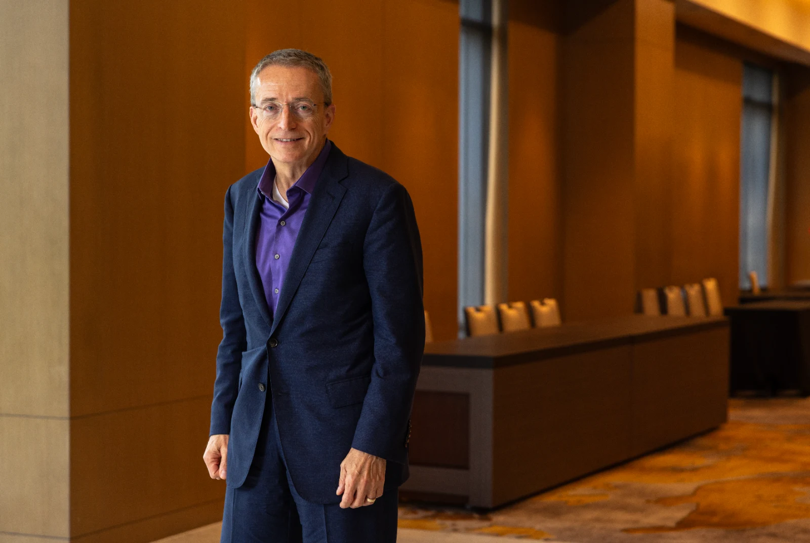
Source:Kuan Hsieh
The former Intel CEO says demand for AI is effectively limitless, but physics is not. The startups he backs are attacking memory, packaging, power and copper. All of them need Taiwan’s supply chain to succeed.
Views
Pat Gelsinger Ranks AI’s Next Bottlenecks — and Sends His Startups to Taiwan to Break Them
By Elaine I-yun Huangweb only
“How much AI do we want?” Pat Gelsinger asked during an interview with CommonWealth Magazine in Taipei in October, his first visit in a year. His own answer: ten thousand times more.
He wants every business process infused with intelligence, and every process step on every production line in Taiwan checked by AI. “I don’t want to sample the manufacturing line. I want to have a hundred percent,” he said. “When I have a field failure, I want to be able to say exactly which machine, on which device, on which day, led to that field failure.”
But can the world supply 10,000 times the power, 10,000 times the memory, 10,000 times the wafer fabs? “Impossible,” he said, spreading his hands.
The world’s electric grid grows only 4% to 5% a year, and about half of that new supply already goes to AI data centers. AI, Gelsinger argues, must become at least 10,000 times more efficient. Making a chip 10% better, he said, is meaningless.
That gap between limitless demand and finite physics is where the next AI battle will be fought. Gelsinger, a 46-year industry veteran who was an architect of Intel’s 386 and 486 processors and later its CEO, is now a general partner at Silicon Valley venture firm Playground Global. He is betting on a cluster of startups built to tear down these walls. Behind every wall stands a Taiwanese supply-chain partner.
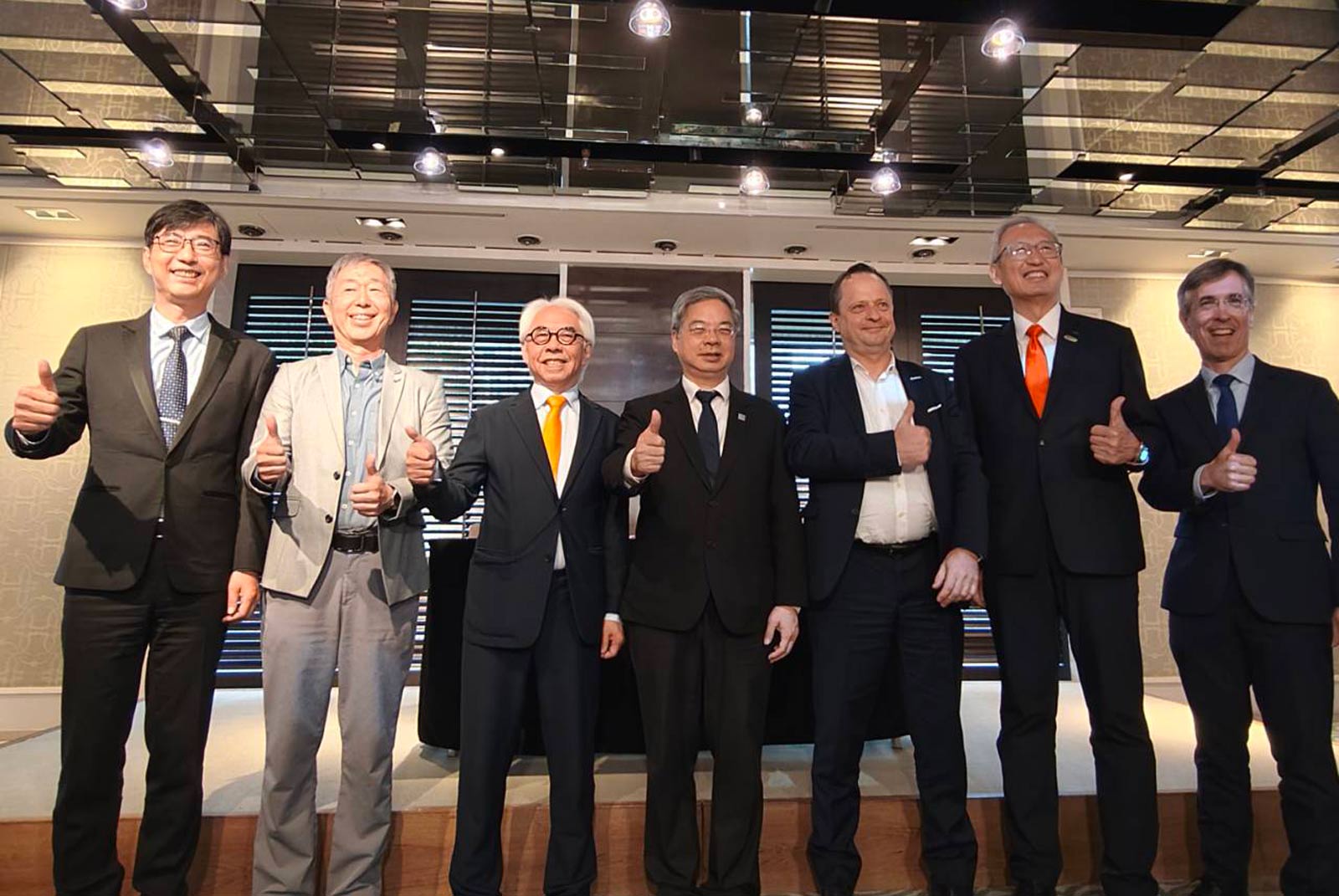
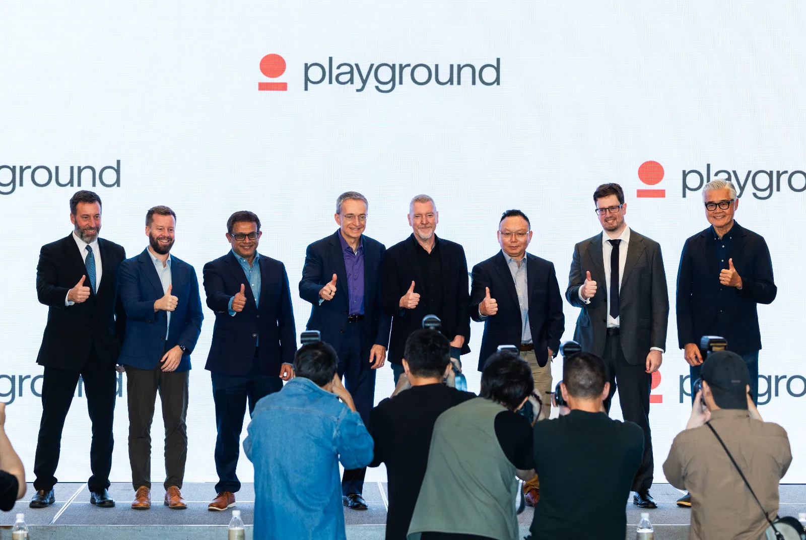 On Oct. 27, Playground held a press event in Taipei, where Gelsinger brought his portfolio companies to meet Taiwan’s manufacturers.
The bottleneck keeps moving
Where are the walls? In an interview with venture firm a16z, Gelsinger noted that AI can shrink chip design to three months, while wafers, packaging and rack integration still take nine. When one thing gets easier, the bottleneck moves somewhere else.
He laid out the order. A year ago, leading-edge logic wafers were the biggest constraint. “I think the biggest one today is memory,” he said. “The biggest one tomorrow is probably advanced packaging, and then power delivery.” Around 2028 and 2029 comes the big conversion from copper to optical, “and then we’ll be fighting the supply chains” for optical components such as lasers and modulators.
The unit of thinking has changed, too. The industry used to talk about a single chip. Now it talks about a whole system, and the unit is the rack.
Systems thinking is not new. Gelsinger took part in many industry discussions on system-level integration (SoIC). But most were “bottom up,” he said, looking from the chip to the package to the next layer of the system. Seen from the chip, any new technology that adds cost or complexity tends to be judged not worth it.
AI flipped that order. Companies now start by committing US$50 billion to a 1-gigawatt data center and work downward. “Five percent of a fifty billion dollar investment is still billions of dollars,” he said. A technology that looks too expensive or complex at the chip level becomes worth doing if it saves 5% across the whole data center.
He pointed to 800-volt direct current (800VDC) power for AI data centers. “Jensen and I argue on things occasionally,” he said of Nvidia CEO Jensen Huang. “One thing we agree upon is that the data center of the future will become an 800 volt DC.” No single component would redesign itself for that. But once the unit is the rack, changing how power is distributed forces every component inside to change. In the same way, a shift to all-optical switching will push co-packaged optics down to the chip level.
“Jensen is not building a GPU. He now says my unit is a rack,” Gelsinger said. “And in the future, he will say his unit is a data center.”
A ‘hideous memory’
AI is a memory workload, Gelsinger says. Yet high-bandwidth memory (HBM), the component propping up the AI boom, is in his words a “hideous memory.”
He lists three charges. First, producing 1 gigabyte of HBM takes four times the silicon of conventional memory, crowding out chips for phones and PCs. “So your iPhone’s price just went up,” he said. Second, data can only enter and leave through the chip’s edge, its “shoreline.” “Essentially, I’m sucking on a straw,” he said. Third, DRAM does not like heat, and stacking it creates “a thermal sandwich.”
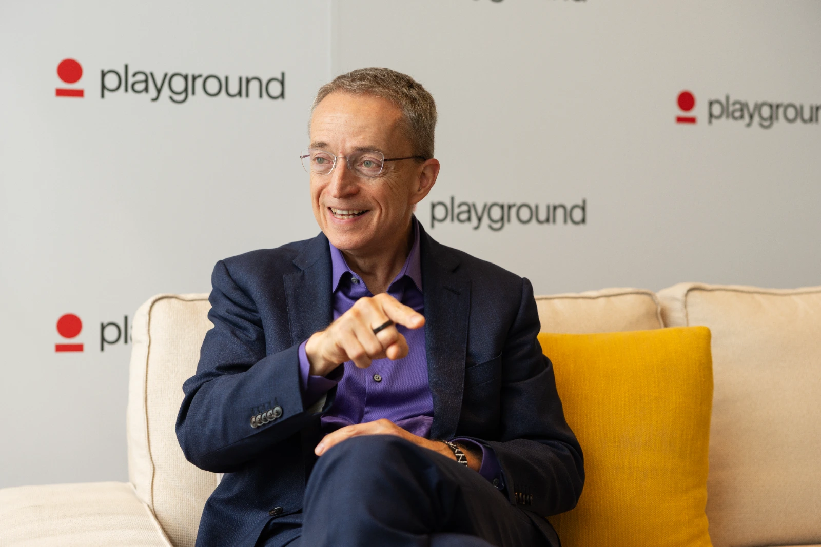
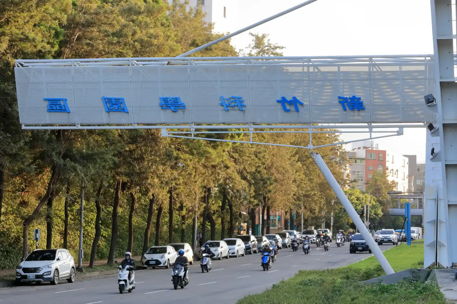 Pat Gelsinger is bringing Silicon Valley startups to Hsinchu to secure manufacturing capacity. (Photo: Chien-Ying Chiu)
The deeper problem: “How many major new memory technologies have there been in the last thirty years? Zero.”
There are two ways through this wall. One is to invent a new kind of memory that neither eats so much silicon nor fears heat. The other is to keep the memory but move it, placing it directly on top of the compute chip and pulling out the straw. Gelsinger has bet on both: one company just launched, the other is about to ship.
The first is Nagare Labs, which debuted at Playground’s Taipei event. “I originally thought training was the hard part and inference was the easy part. That turned out not to be the case at all,” said co-founder Suman Datta.
Agentic AI keeps stretching context windows, making data movement the bottleneck. Nagare uses oxide semiconductors to build a memory cell with two transistors and no capacitor, combining the speed of SRAM with the density of DRAM. Crucially, it tolerates heat. Heat sensitivity is what turns HBM into a thermal sandwich, but Nagare’s material “can be stacked directly on top of logic chips,” Datta said — removing both the straw and the sandwich.
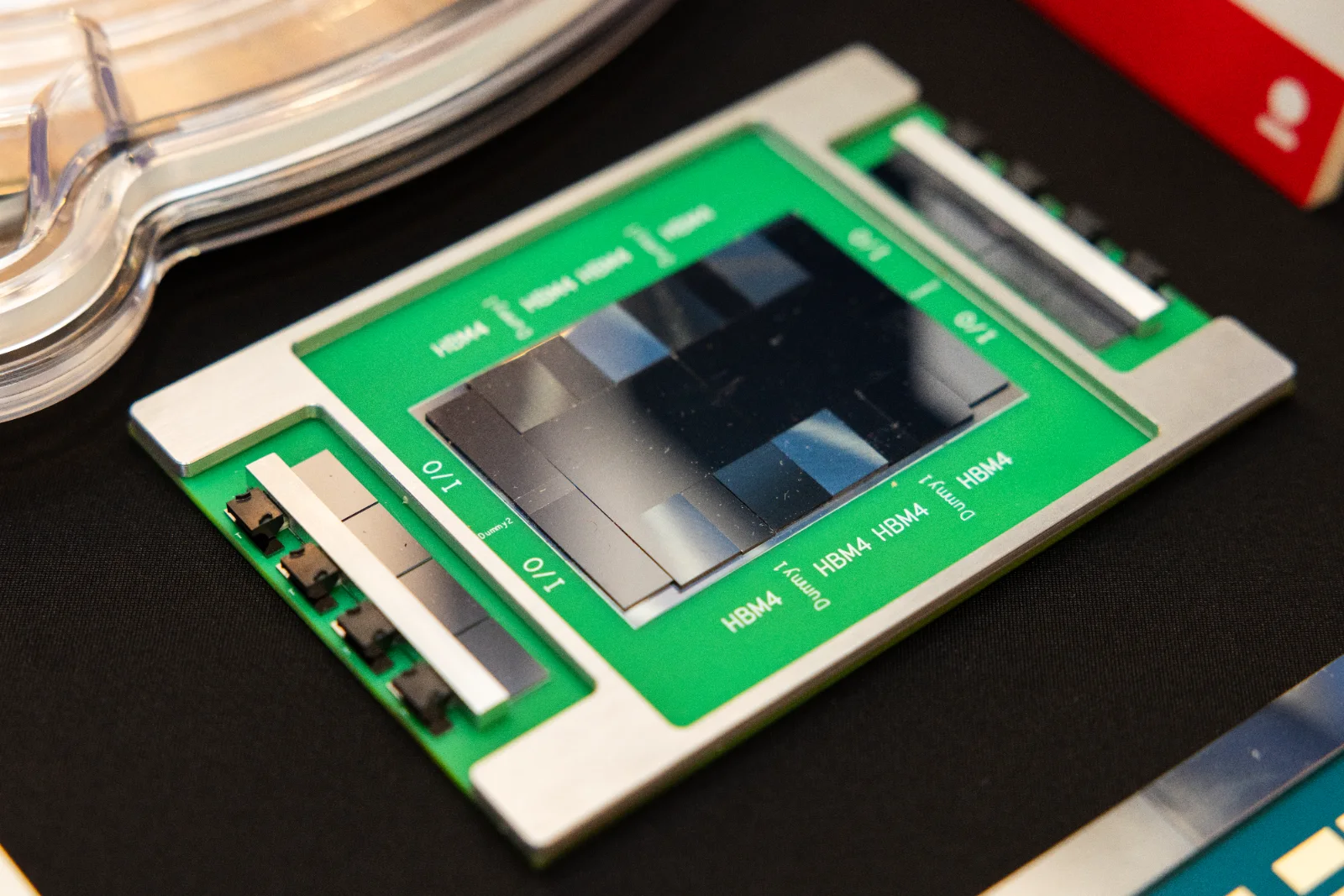 Ayar Labs specializes in co-packaged optics (CPO) technology.
This is also Gelsinger’s most personal bet. Datta began his career at Intel, where he worked on several generations of logic transistor technology. “This is the best transistor team at Intel,” Gelsinger said. “They took high-K metal gates into manufacturing.” The team has refined the technology for seven or eight years and is now seeking a foundry partner, which brought it to Taiwan.
The second path, d-Matrix, is already in production. Its first-generation product computes directly inside the SRAM of a TSMC 6-nanometer chip and has shipped in full racks to cloud providers. The second generation goes straight at the straw problem, stacking custom DRAM on top of a TSMC 4-nanometer logic chip.
“HBM sits to the side, so data can only come out the edge. We stack the DRAM directly on top, so the whole array can be accessed,” a d-Matrix vice president explained. For inference, that determines speed, because the time to generate each token is what matters — “that’s memory bandwidth.”
Gelsinger calls this “near-memory computing,” with bandwidth coming from the full plane rather than the shoreline. D-Matrix’s second-generation chip has just taped out, will be demonstrated in about three quarters, and will go into Nvidia’s MGX racks.
Both approaches pull memory tight against compute. And both companies have come to Taiwan: d-Matrix manufactures at TSMC, and Nagare plans to bring its technology onto 12-inch production lines next year.
“Taiwan is clearly the best place,” Datta said.
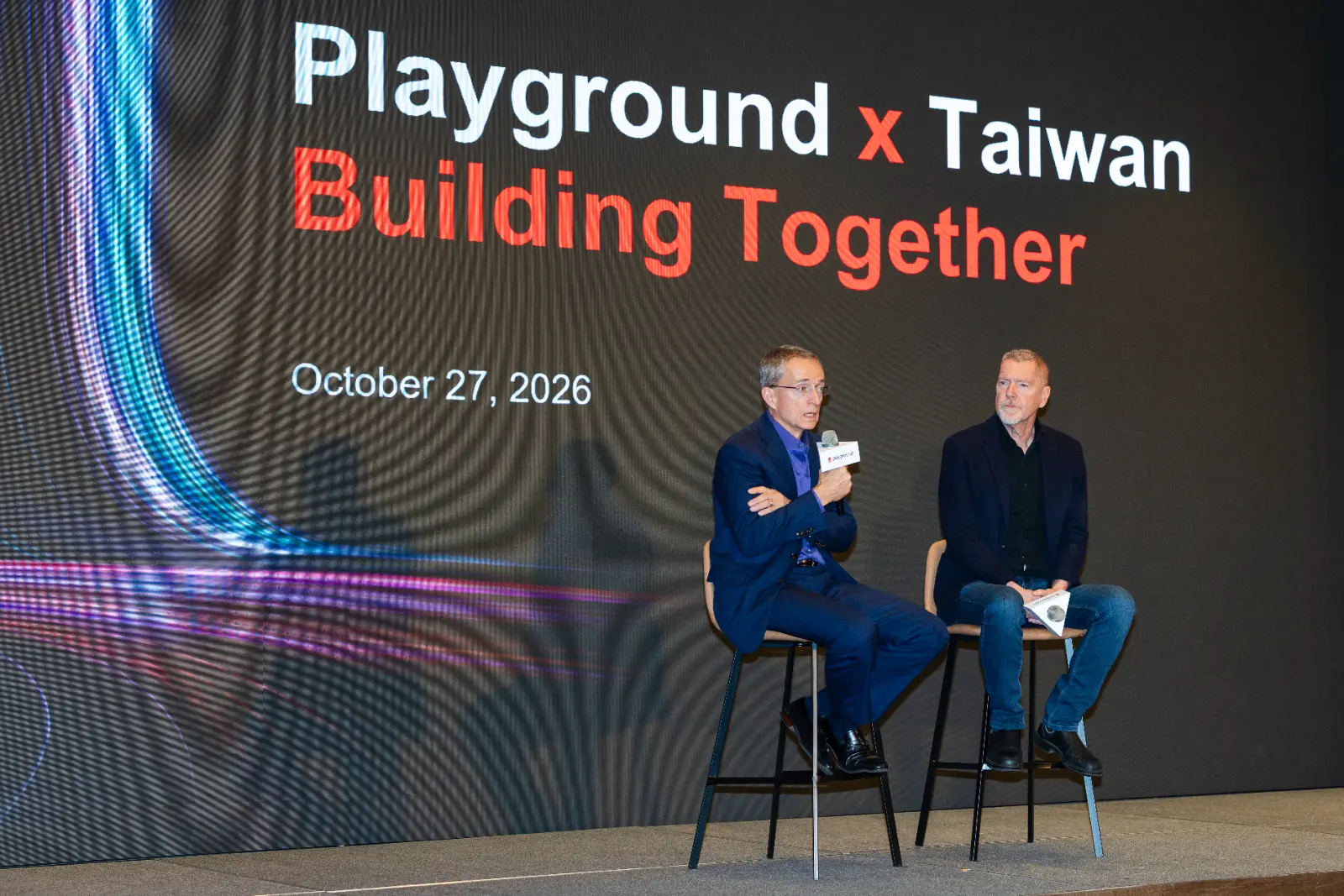 Playground Global general partner Pat Gelsinger brought the venture firm’s portfolio startups to Taiwan to deepen collaboration with local manufacturing partners. (Photo: Kuan Hsieh)
Three more walls
Beyond memory, Gelsinger’s ranking has three more bottlenecks, and his calls on each are blunt.
Advanced packaging is “tomorrow’s” bottleneck — “a bigger limiter than leading logic wafers for the next several years,” he said. An AI chip is no longer one chip; compute, memory and power components must all be integrated into a single package. Packaging and testing once made up only about a tenth of the bill of materials, and chip architects like him “didn’t care at all,” he admitted. Now it determines performance and yield.
Power will become the most fundamental constraint. Global grid capacity grows only 4% to 5% a year, and half the increase already goes to AI. Electricity must also be stepped down layer by layer on its way to the chip. “If I have a 2,500 watt chip, that needs 6,000 watts of power,” he said. His bold bet here is PowerLattice, which puts the final voltage-regulation stage directly inside the GPU package. It says this can cut compute power consumption by half, letting data centers deliver more computing on their existing power supply — a direct hit on today’s hottest data-center pain point.
The last wall is optics, a field Gelsinger has followed for 25 years, because copper has hit its physical limits. Copper carries high-speed signals only a few meters, so GPUs must be crammed into a single rack, dense and hot. Getting Nvidia’s NVL72 rack to work and scale, he said, had “every engineer in Taiwan” working all night and every weekend for about a year and a half. “It was a nightmare.” That, he said, is what fighting physics looks like.
Optics changes the equation. “My cable lengths can only be four meters long. Let’s make them twenty meters. Let’s spread them out. Let’s make the thermal problems easier,” he said. GPUs could then link across racks into clusters of a thousand or more. He expects the tipping point in 2028 and 2029. But optics depends on lasers, and the next wall is already visible: “We don’t have enough indium phosphide fabs in the world.”
Prototype at lunch, production at dinner
Gelsinger first came to Taiwan more than 40 years ago with then-Intel CEO Andy Grove. To him, Taiwan is where you get a “prototype at lunch” and “production at dinner.” “That doesn’t happen if you’re in the U.S.,” he said. On this trip he again visited old friends at TSMC, Foxconn and MediaTek.
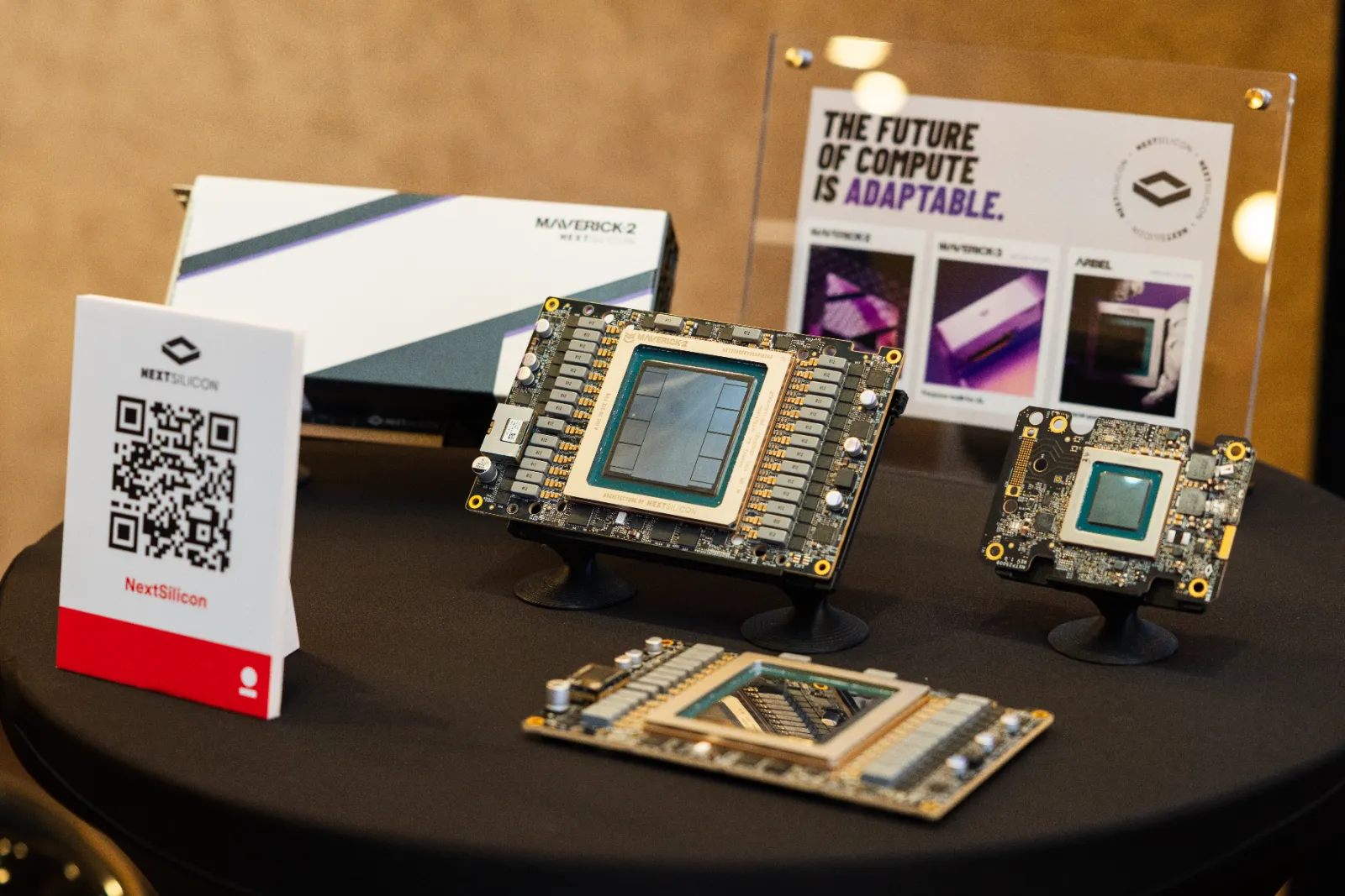 NextSilicon’s Arbel CPU chipset. (Photo: Kuan Hsieh)
More surprisingly, he said he wants all of his portfolio companies to set up in Taiwan. “Part of the reason I’m bringing the companies here is because I think they all need offices here,” he said, “because the supply chain of the world is here.”
Ayar Labs, PowerLattice and d-Matrix are already building teams in Hsinchu, the heart of Taiwan’s chip industry. A local presence, Gelsinger said, means “our companies get to be more influenced by Taiwan, but also get to be more influential with Taiwan.”
“Over the past two years, I’ve been in Taiwan almost every week,” said Ayar Labs co-founder and CEO Mark Wade. The company announced its Taiwan presence last year; its office in Zhubei, next to Hsinchu, is finished and set to open early next year. The local team now numbers about 10 and will grow over the next one to two years to work closely with Taiwanese manufacturers. The reason is simple, Wade said: to bring new technology into high-volume production, “Taiwan is the center of the universe.”
When d-Matrix was founded in 2019, its first Taiwanese partner was TSMC, followed by Alchip and Wistron. One executive said he visits Taiwan every two months; a colleague added, “Soon it’ll be every week.” D-Matrix hired its first Taiwan employee in Zhubei in September, “with more coming next month.” He noted that Gelsinger’s deep ties to Taiwan’s supply chain are critical. With global capacity tight, a startup’s biggest challenge is getting “the right level of attention” and foundry capacity — and Gelsinger “can help Taiwanese companies understand why a company like d-Matrix matters.”
Not a bubble but a supercycle
In Washington, scrutiny of frontier AI models has raised talk of an AI slowdown driven by rules and regulation. Is Gelsinger worried the tide is turning?
 Silicon Valley venture capital firm Playground Global held its “Co-Creating the Next Era of Computing” press conference in Taipei on Oct. 27, where general partner Pat Gelsinger said the AI boom is far from over.
He shook his head. “We believe we have two decades of an innovative cycle in front of us yet,” he said. Moving from large language models to reasoning models raised computing needs about tenfold. “Are we done with our innovations and models? Absolutely not.” There will be corrections along the way. Small earthquakes are good, he said; it is the big ones that are bad.
Flawed models do need oversight and fixing, he said. He drew on chipmaking: at Intel, about 60% of the cost of developing a microprocessor went into creating the chip and 40% into testing it. If AI developers spend 90% on building a model and 10% on testing, “I say not okay.” An untested model could one day take down a power grid or a hospital. His message to model makers is direct: “Do your job.” If they don’t make the models good, “governments must step in.”
Asked why he keeps making bold bets on frontier technologies with uncertain prospects, Gelsinger laughed. “My companies are brave, and I’m happy to join them.”
Having ranked the bottlenecks and placed his bets, Gelsinger made the reporter a promise: “When we’re sitting together next year, we can check to see if I was right.”
Have you read?
- Why TSMC Is Seeking Rare-Earth-Free Equipment as China Tightens Its Grip
- Nvidia Turns to Samsung to Shake Up the AI Substrate Market. Unimicron and Kinsus Face a New Threat
- From Sugar to Semiconductors: The Price Taiwan Keeps Getting Wrong
Uploaded by Ian Huang
Views

Subscribe to CWE Newsletter (every Thursday)
Stay abreast of what's happening in Taiwan with our weekly digest.
Keywords: