Why TSMC Is Letting Go of CoWoS—and Where Its Real Second Moat Lies
Source:Shutterstock
CoWoS has long been regarded as one of TSMC’s greatest competitive advantages in the AI era. But recent comments from the company suggest it may not see advanced packaging as its true moat after all. If not CoWoS, then what is TSMC’s real second moat?
Views
Why TSMC Is Letting Go of CoWoS—and Where Its Real Second Moat Lies
By Liang-rong Chenweb only
Three months ago, this newsletter exclusively revealed that Douglas Yu(余振華), an Academia Sinica academician and former TSMC vice president of R&D best known for developing CoWoS, would join MediaTek as an adviser after retiring.
He was expected to help MediaTek overcome its biggest challenge at the time—the poor yields of Intel’s EMIB-T 2.5D packaging technology, which MediaTek is using for the second TPU it is helping Google develop.
The sensitive news caused a stir. Yu himself received numerous inquiries from former colleagues asking why he would go help a rival—Intel.
MediaTek also quickly issued a statement clarifying that Yu would not be involved with EMIB-T.
Then, at TSMC’s July earnings call, there was a surprising turn of events.
When TSMC President C.C. Wei(魏哲家) was asked what he thought about customers switching to EMIB-T, he said: “Welcome.”
“We hope they succeed so they can share some of the burden,” he explained. TSMC’s CoWoS packaging capacity is so tight that it is actually constraining customers’ growth, so the company is happy to see alternative packaging solutions emerge. “That actually helps our front-end business.” (By allowing TSMC to sell more 3nm and 2nm chips.)
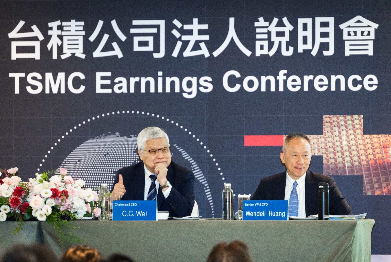
In a report issued after the earnings call, Bernstein said Wei’s attitude showed that TSMC does not actually regard advanced packaging as a “moat.”
That is despite the explosive growth of its CoWoS revenue, which made TSMC the world’s largest semiconductor packaging company last year.
Fundamentally, however, senior management only wants to pioneer a new path as a demonstration, encouraging OSAT providers to follow suit. Once they roll out various “CoWoS-like” solutions, TSMC is happy to hand some of the orders over to them.
That surprised me. I had always viewed advanced packaging technologies led by CoWoS as TSMC’s “second moat,” alongside its advanced process technology.
After all, CoWoS has a nearly 100% share of the AI chip market, even higher than TSMC’s share of advanced-node manufacturing.
For example, Nvidia’s most advanced GB200 GPU currently uses a 4nm process, two generations behind the leading edge and one that Samsung can also provide. Yet Nvidia places 100% of its orders with TSMC because it needs CoWoS packaging to enable ultra-high-speed connections between the GPU and memory.
To me, this is clear evidence of TSMC using “advanced packaging to lock in advanced-node manufacturing.”
What is more, Moore’s Law has slowed from a new generation every two years in the past to one every three years, with further progress becoming increasingly difficult. Many believe that advanced packaging, which places multiple chips in close proximity or even stacks them vertically, will be the primary driver of continued semiconductor performance gains going forward.
Is CoWoS Really a Moat—or Just a Ditch?
The closing passage of a famous 2024 article in IEEE Spectrum, “How We’ll Reach a 1 Trillion Transistor GPU,” co-authored by then-TSMC Chairman Mark Liu(劉德音) and Chief Scientist H.-S. Philip Wong(黃漢森), best captures this mindset:
“For the past 50 years, semiconductor technology has been like walking through a tunnel, with a clear path and direction. Everyone knew there was only one thing to do: shrink transistors. Now we have emerged from the tunnel.....There are more possibilities ahead, and we are no longer constrained by the past.”
(To read this exclusive story in full, visit the Tech Taiwan Substack)
Views

Subscribe to CWE Newsletter (every Thursday)
Stay abreast of what's happening in Taiwan with our weekly digest.
Keywords: